
Master PCB Design Using a Proven 12-Step Industry Framework
Learn PCB Design systematically — from requirements to manufacturing — using practical workflows developed across automotive, industrial, IoT and embedded products.
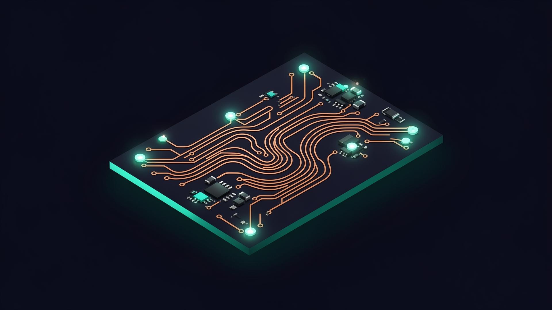
Get the free guide and join our WhatsApp Channel for continuous PCB & Hardware Design learning.
HDProEx 12-Step PCB Design Execution Framework
A practical industry workflow followed by PCB teams from design input analysis to final manufacturing output release.
This 12-step PCB design process gives a structured path from understanding design inputs to generating final manufacturing outputs. It helps ensure the board is electrically correct, mechanically fit, manufacturable, assembly-ready, and properly released.
Step description
Collect all required design inputs, understand project scope, review schematic, analyze BOM, study mechanical constraints, identify critical components and nets, clarify missing information, align teams, prepare checklist, and freeze the design baseline.
Step 1 of 12
Why It Works
Engineered for real-world PCB projects
Structured Workflow
A repeatable path from requirements to release — no guesswork.
Industry Best Practices
Rules distilled from automotive, industrial and embedded products.
Reusable Process
Apply the same framework across boards, teams and product lines.
Fewer Design Errors
Built-in checks catch issues before they reach the fabricator.
Manufacturing Focus
Designs released with complete, unambiguous fab packages.
Career Growth
Think like a senior PCB engineer from your very first project.
Free Resource
Get The FREE PCB Design Guide
A compact, practical handbook covering the foundations every electronics engineer should know before touching a layout tool.
- PCB Design Process
- PCB Materials
- Stackup Basics
- Placement Basics
- Routing Basics
- Manufacturing Basics
Stay Connected with HDProEx
Enjoying this guide?
Join the official HDProEx WhatsApp Channel to receive PCB Design tips, Hardware Design insights, engineering checklists, industry updates, new tools, and future free resources.
- PCB Design Tips
- Hardware Design Insights
- Engineering Checklists
- Career Growth Advice
- Industry Updates
- New Tool Announcements
- Free Learning Resources
- HDProEx Community Updates
Starter Bundle
PCB Design Starter Bundle
Everything you need to start designing production-grade PCBs — one bundle, one price.
What you get
- Worth ₹2,999Full Access of PCB Design Process
- Worth ₹2,99912D Hardware Design Framework
- Worth ₹1,499Design Checklist
- Worth ₹2,999Engineering Tools Suite
- Worth ₹1,999Component Engineering Guide
- Worth ₹1,999PCB Interview Mastery Challenge™Coming Soon
Total Value
₹14,494
Limited Launch Offer
₹399
₹999
Lifetime Access
Launch Offer Price. Price will increase after new tools and assessment modules are released.
🔥 Launch Offer – Limited Time
One-time payment · Instant access · Lifetime updates
What's Inside
Explore What’s Inside the Bundle
Each premium resource is designed to help you learn, apply, verify, and build real PCB and hardware design skills.
PCB Design Process
Learn the complete 12-step PCB design flow from input analysis to output generation.
12D Hardware Design Framework
Understand how professional engineers move from idea, requirements, architecture, design, prototype, debug, and next revision.
Complete PCB Design Checklist
Use a professional stage-by-stage checklist to verify PCB design quality from input review to final manufacturing release.
Engineering Tools Suite
Access practical workflow tools, PCB calculators, readiness analyzers, datasheet assistants, library validation tools, DRC analyzers, and release readiness checkers.
Component Engineering Guide
Learn how to review datasheets, identify packages, verify libraries, and prepare components for PCB design. Includes the Component Engineering Intelligence Tool — generate engineering reports from any part number.
PCB Interview Mastery Challenge™
A gamified PCB interview preparation platform featuring levels, missions, XP points, badges, interview readiness scoring, and technical challenges. Currently being updated and will be available soon.
Roadmap
Your Learning Journey
A guided path from PCB fundamentals to a complete hardware design skill set.
Step 1
PCB Design Process
Step 2
12D Hardware Design Framework
Step 3
Component Engineering Guide
Step 4
Engineering Tools Suite
Step 5
Design Verification Checklist
Step 6
PCB Interview Mastery Challenge
Coming Soon
Toolkit
HDProEx Engineering Toolkit
Practical PCB workflow tools mapped to each step of the PCB Design Process.
Featured Engineering Tools
Input Readiness Score
Step 1 – Getting & Analysing Inputs
Check whether schematic, BOM, mechanical files, constraints and baseline inputs are ready before layout.
Open ToolLibrary Readiness Analyzer
Step 2 – Component Library Creation
Analyze component library readiness, datasheet information, missing footprints, symbols and 3D model status.
Open ToolPlacement Readiness Score
Step 6 – Component Placement
Evaluate mechanical drivers, critical components, power blocks, signal flow, power flow and assembly fit.
Open ToolRelease Readiness Checker
Step 12 – Output Generation
Confirm Gerbers, drill files, fabrication docs, assembly docs, verification files and final release package.
Open ToolCommunity
Join The HDProEx Community
Connect with engineers building real PCBs across automotive, industrial, IoT and embedded products.
- Weekly PCB Tips
- Career Guidance
- Design Reviews
- Industry Discussions
- Templates
- Resources
About HDProEx
Bargunan Ponnusamy
Founder · 18+ Years Industry Experience
Our mission: become the #1 platform for Electronics, Hardware and PCB Design Engineers — a place where engineers level up with structured frameworks, practical tools and a community that ships real hardware.
Start Your PCB Design Journey Today
Pick the step that fits you best — a free guide, the starter bundle, or a community of engineers building real hardware.
Get the free guide and join our WhatsApp Channel for continuous PCB & Hardware Design learning.